Nanoelectronics
The phenomenal growth in the CMOS technology over the past four decades has enabled very high performance compute and storage systems, powering the information technology revolution. The MOS transistor has meta-morphed from a few 10s of microns dimension in 1970s to a few 10s of nano meters today. Semiconductor memory and high performance logic circuits have been the technology drivers to architect the miniaturization of the MOS transistor and this will continue in the foreseeable future. The underlying premise of this growth is the ability to miniaturize the MOS transistor dimension by 30%, in every two year cycle on an average [1].
The scaling of MOS transistor in Nanoelectronics era, necessitates the exploration of new materials (high-k gate dielectrics such as HfO2, Er2O3, Gd2O3; new channel materials such as Germanium, III-V and Graphene) and new device structures (Double gate FET, FinFET, Schottky source/drain FET). The facilities available at the centre provide an opportunity to carry out both experimental research and design and modelling research for Nanoelectronics devices. There are several groups in the Institute, working on various aspects of synthesis of new materials, processing techniques, device structures, modelling and simulation. Some recent highlights from the centre are summarized below. This is just a representative sampling, and not an exhaustive list of topics.
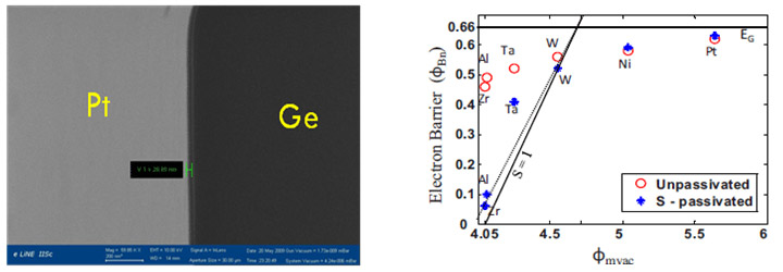
Schottky junction transistors could provide a solution for ultimate scaling of junction depths, by replacing diffused junctions. However, Fermi level pinning in Silicon and Germanium makes it difficult to create schottky junctions on p-type substrates. This problem arises due to surface states at semiconductor interface. We have been able to use sulfur passivation on Germanium substrates to achieve ideal schottky junctions (Fig.1). Through sulfur passivation, the low work function metals (such as Al, Zr) are able to provide rectifying behaviour on p-type Germanium and ohmic behaviour on n-type Germanium [2]. This opens up the possibility of schottky junction NMOSFET devices.
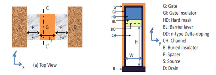
HEMT device structure, traditionally used in III-V materials provides very high carrier mobilities and on current, but suffers from high off current as well. We propose a hybrid device structure HFinFET, a hybrid transistor structure on III-V nanowire structure, which combines the high on current property from HEMT structure along with the excellent gate control and off current from FinFET structure (Fig. 2). The gate to source/drain underlap length can be tuned appropriately [3,4] to obtain the speed-power performance as per the requirements of ITRS.
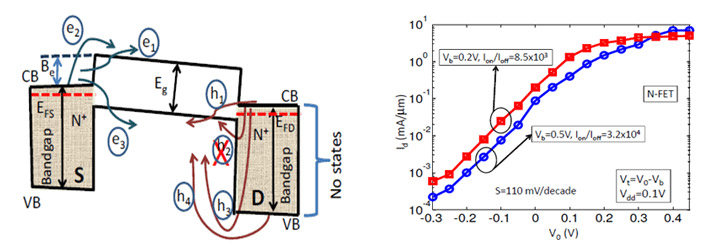
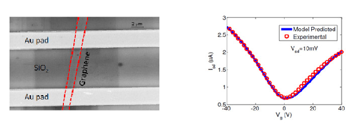
Graphene, a monolayer of Carbon atoms arranged in hexagonal lattice with honeycomb pattern, has created a large interest for potential application in Nanoelectronics. The greatest advantage for nanoelectronics applications, is the fact that Graphene is amenable for planar technology. Graphene has a very unique band structure with linear energy-momentum dispersion, resulting in extremely high carrier mobility. While Graphene has very high mobility, it also suffers from zero bandgap, thus making it very difficult to get a well behaved transistor. In particular, it will not be possible to turn off the MOSFET and hence the typical on current to off current ratio (Ion/Ioff) have been less than 10. This should be contrasted with typical Silicon MOSFET which has Ion/Ioff greater than 10,000. Fig. 3 shows backgated Graphene transistor with SiO2 gate dielectric, realized in our Nanofab through exfoliation technique. The corresponding I-V characteristics illustrate the ambipolar nature of the device with Dirac point very close to Vg=0V. An in-house model is developed to model the transport, and the model predicted characteristics match the experiment fairly well. It can be seen that the Ion/Ioff ratio is less than 5.
Several techniques have been proposed to open bandgap in Graphene. It has been demonstrated, both theoretically and experimentally, that Graphene Nanoribbons (GNR) show bandgap which is inversely proportional to their width. GNRs with about 20nm width have bandgaps in the range of 100meV. But it is very difficult to obtain GNRs with well defined edges. An alternate technique to open the band gap is to use bilayer Graphene (BLG), with an asymmetric bias applied in the direction perpendicular to their plane. Typical bandgaps of 200meV are obtained for fields in the range of 107 V/cm. The MOSFET on BLG Graphene have resulted in Ion/Ioff of about 100. This is still inadequate for typical digital CMOS applications. We have proposed a transistor structure with silicon source/drain junctions in conjunction with Graphene channel to enhance Ion/Ioff ratio [5]. In a typical Graphene transistor with metal source/drain junctions, the high off current is because of hole tunnelling from the drain region into the channel. By using Silicon source/drain junctions, the tunnelling component of hole current can be completely shut-off resulting in an Ion/Ioff ratio of more than 10,000. This is illustrated in the simulation predicted results in Fig. 4.